A Brief History of Silicon as a Semiconductor
Silicon was discovered in the early half of the 19th century by Jöns Jacob Berzelius, a Swedish chemist. After its discover, there were no major uses for over 100 years, until the digital revolution. While silicon makes up about 95% of all semiconductors today, germanium (Ge) made up most of the original semiconductors and transistors. After finding that silicon has superior thermal and leakage properties than Ge in 1954 by Texas Instruments, the industry movement began. Fast forward to today, and there are 10.5 billion square inches of silicon wafers shipped around the world each year. These power nearly everything we use on a daily basis from phones to cars. There are also countless unique research purposes that are pushing technological boundaries.
Description-ingot

silicon ingot
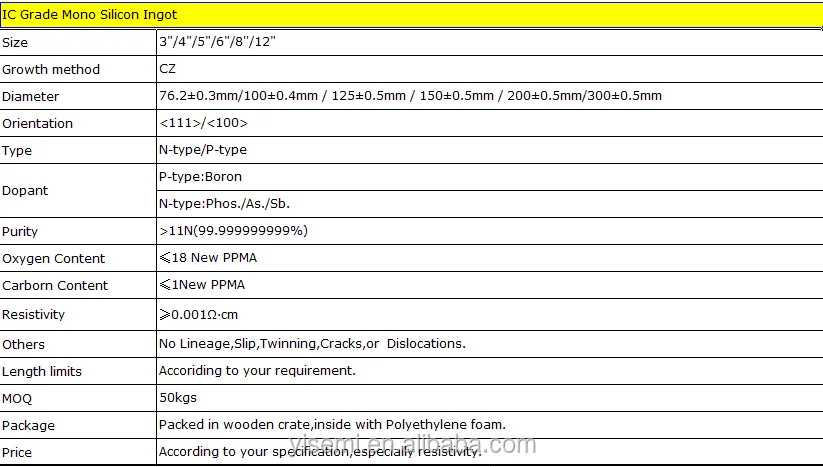
Growing a silicon ingot can take anywhere from a week to an entire month depending on many factors including size, quality and specifications. More than 75% of all single crystal silicon wafers grow via the Czochralski (CZ) method which uses chunks of virgin polycrystalline silicon. These chunks are melted down and placed in a quartz crucible along with small quantities of elements called dopants, the most common of which are boron, phosphorus, arsenic and antimony. The added dopants give the desired electrical properties for the grown ingot and depending on which dopant is used, the ingot becomes a P or N type ingot (boron: P type; phosphorus, antimony, arsenic: N type).
Yisemi can currently produce 76mm and 300mm silicon ingot, as well as custom diameters between 50mm and 400mm.
Why choose me?
- Yisemi is the largest factory of silicon wafers/ingots in the world.
- We have a multi-million dollar inventory of wafers ready to ship.
- We deliver in just 1 day in the U.S. and around the world in 3 days.
- All products are sold at or below market price.
- Yisemi has a 99%+ on-time delivery record.
- We have been successfully supplying wafers worldwide for 25+ years.
- All products are manufactured by the Our factory.
- Yisemi is a wafer processing 1-stop shop: thermal oxide to lithography.
- We never charge a premium for anything.
- Yisemi is an ISO 9001:2008 Certified Company.
FAQ
Q1. Can I have a sample order for wafer?
A: Yes, we welcome sample order to test and check quality. Mixed samples are acceptable.
Q2. What about the lead time?
A:Sample needs 3-5 days, mass production time needs 1-2 weeks for order quantity more than
Q3. Do you have any MOQ limit for led light order?
A: Low MOQ, 25pc for sample checking is available
Q4. How do you ship the goods and how long does it take to arrive?
A: We usually ship by DHL, UPS, FedEx or TNT. It usually takes 3-5 days to arrive. Airline and sea shipping also optional.
